
From Micro-area Thin Films to Sub-nanometer Heterostructures: Polycapillary X-ray Optics Empowering XRF Analysis of Semiconductor Thin Films
This article focuses on several capabilities required for semiconductor thin film analysis: high-throughput micro-area excitation, depth-resolved analysis of layered structures, low-background particle detection, in-situ observation of solid/liquid interfaces, and ultimately the identification of sub-nanometer ultra-thin layers in semiconductor heterostructures.
Click the blue text
Follow us
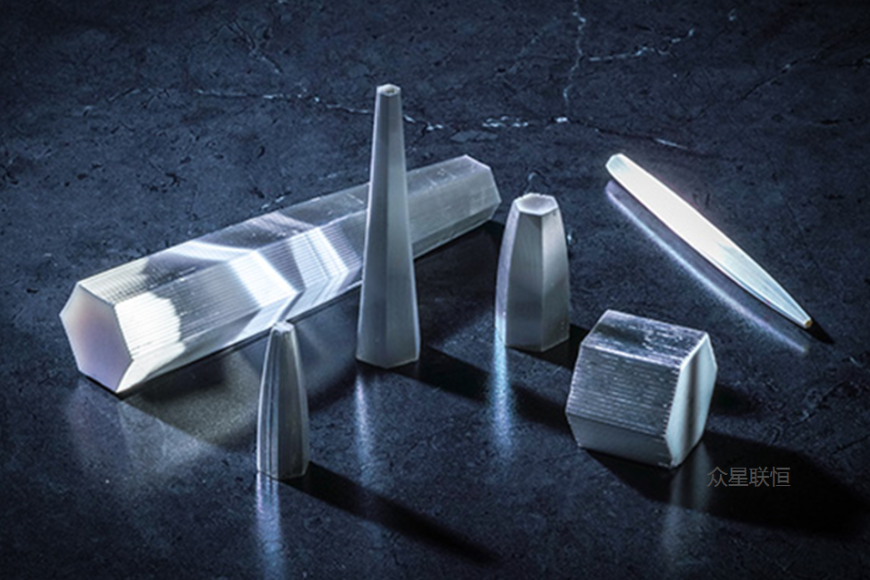
Figure 1. Physical image of a polycapillary X-ray lens
As semiconductor devices move toward smaller linewidths, more complex heterostructures, and more multilayer film stacks, thin film characterization faces not only the challenge of "measuring accurately" but also "measuring accurately under micro-area, non-destructive, and low-background conditions." From metallization layers, barrier layers, and packaging coatings to sub-nanometer interfacial layers in epitaxial heterostructures, researchers need to simultaneously address elemental composition, thickness variations, interlayer distribution, and localized contamination.
Polycapillary X-ray lenses are precisely the key optical components in such micro-area XRF and confocal XRF systems. Taking the polycapillary X-ray lenses from XOS, a partner of Top Unistar, as an example, they consist of a large number of hollow glass capillaries with smooth inner walls, which utilize total external reflection of X-rays to focus a divergent beam into a micron-sized, high-flux focal spot. Compared with traditional pinhole collimation, polycapillary lenses can increase the photon flux density at the focal spot by several orders of magnitude, thereby providing the hardware foundation for micro-area, depth, and low-concentration analysis of thin film samples.
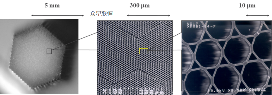
Figure 2. Cross-sectional micrograph of a polycapillary X-ray lens
Based on this concept, this article will elaborate on several capabilities required for semiconductor thin film analysis: high-throughput micro-area excitation, depth-resolved analysis of layered structures, low-background particle detection, in-situ observation of solid/liquid interfaces, and ultimately the identification of sub-nanometer ultra-thin layers in semiconductor heterostructures. Through these references, it can be seen that the value of polycapillary X-ray lenses lies not only in "making the signal stronger," but also in advancing laboratory XRF toward smaller spot sizes, lower backgrounds, and more complex sample environments.
High-throughput Micro-area Excitation and Depth Profiling:
Fundamental Capabilities for Layered Thin Film/Coating Analysis
Semiconductor thin film analysis must first address two fundamental issues: one is compressing the laboratory X-ray source into a sufficiently bright and small micro-area excitation beam; the other is distinguishing elemental signals from different depths in multilayer films, metallization layers, packaging coatings, or barrier layers as much as possible. The study by Smolek et al. starts from system performance and demonstrates how polycapillary optics enhance the usability of micro-area analysis and depth profiling of layered structures in confocal micro-XRF.
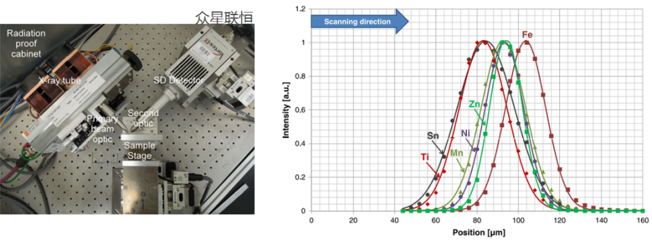
Figure 3. Confocal micro-XRF systems compared by Smolek et al. and depth profiling results of a multilayer automotive coated steel sheet. The left image shows the actual optical path of the Osaka City University system, and the right image shows the results of elements such as Ti/Sn, Mn/Ni/Zn, and Fe varying with scanning depth in the coated steel sheet sample.
Smolek et al. compared two confocal micro-XRF systems from Osaka City University and Vienna University of Technology[1]. In the system characterization phase, the researchers used single-element thin film reference samples with a thickness of 500 nm to evaluate depth/spatial resolution, and used NIST multi-element glass standards to evaluate detection limits; in the application validation phase, non-destructive depth profiling was further performed on pigment layer samples and automotive coated steel sheet samples. The Osaka City University system employed XOS polycapillary optics at both the source and detector ends, with a nominal spot size of approximately 10 μm under Mo Kα conditions and an intensity gain of 7700 times. For the multilayer automotive coated steel sheet, the system was able to resolve the depth distribution of Ti/Sn in the upper layer, Mn/Ni/Zn in the intermediate layer, and Fe from the steel substrate at the bottom, demonstrating that the combination of polycapillary focusing and confocal detection volume can advance laboratory XRF toward micron-scale layered structure analysis. In the context of semiconductor thin films, this capability corresponds to non-destructive micro-area depth analysis of metallization layers, barrier layers, packaging coatings, and thicker functional film layers.
Depth Resolution: Layered Structure Analysis Capability of Confocal
μXRF from Multilayer Coatings
Semiconductor thin films are often not single-layer structures but are stacked from multiple layers of materials. Conventional XRF obtains the superposition of signals from all depths within the excitation volume, making it difficult to determine whether a certain element originates from the surface layer, the interface, or a deeper underlying layer. For structures such as multilayer metallization, packaging coatings, and diffusion barrier layers, planar elemental information alone is insufficient; spatial selectivity in the depth direction is equally important.
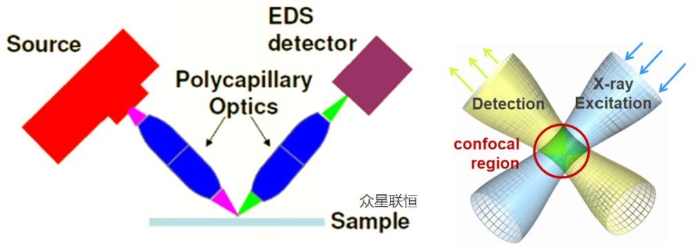
Figure 4. Optical path schematic and principle diagram of confocal μXRF
The research team at Osaka City University constructed a confocal micro-XRF optical path using dual polycapillary lenses[2]. The lens at the source end focuses X-rays into the sample, while the lens at the detector end restricts the detector to receiving fluorescence signals emitted only from a specific spatial volume; when the two focal points coincide, a micron-sized "confocal detection volume" is formed. The actual samples in this study were forensic materials such as automotive paint chips and artificial leather, rather than semiconductor samples; however, it addresses a problem isomorphic to semiconductor thin films: how to obtain elemental depth distributions inside multilayer materials without sectioning. In the experiments, the system achieved a depth resolution of approximately 13.7–22.6 μm and performed non-destructive depth imaging of elements such as Cl, Ti, Fe, Ba, and Zn in multilayer coatings. This result can serve as a methodological reference for depth analysis of semiconductor packaging coatings, multilayer metallization structures, and thicker functional film layers.
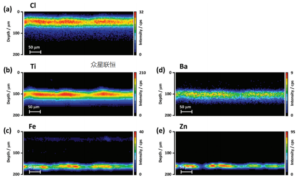
Figure 5. Non-destructive elemental depth imaging of Cl, Ti, Fe, Ba, and Zn in a black paint chip using confocal μXRF.
Low Background and High Sensitivity:
For Particle Contamination and Trace Element Detection in Thin Film Processes
In semiconductor thin film processes, micron-sized particles, metallic residues, and localized contamination can all affect device yield. For such small-sized targets, the detection challenge is not only the low elemental content, but also the high background scattering from the substrate, the small target area, and the tendency for signals to be overwhelmed by surrounding materials. Polycapillary focusing can increase the local excitation intensity, while the confocal configuration can further restrict the detection volume, reducing background from the substrate and non-target regions.
The HORIBA team in Japan compared the performance of conventional capillary μXRF and capillary confocal μXRF (C-M-XRF) in detecting small particles[3]. Conventional μXRF focuses only at the source end and still receives scattering and fluorescence signals from a larger volume; C-M-XRF places polycapillary optics at both the source and detector ends, reading only information from within the confocal volume. This study used small metallic particles and mineral particles on a plastic substrate as targets, focusing on comparing the signal-to-noise ratio and detection limits of the two modes.
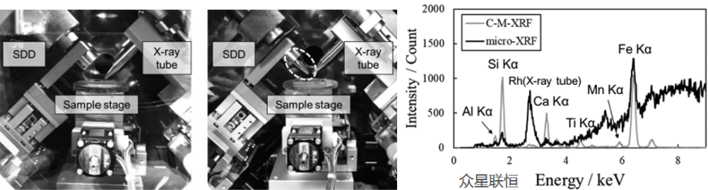
Figure 6. Optical path layouts of μXRF and C-M-XRF and spectral comparison of small particles. The confocal configuration reduces substrate scattering background by limiting the detection volume.
The experimental results showed that in detecting small particles, the confocal configuration significantly improved the signal-to-noise ratio: for Si, the SNR improvement was approximately 14.6 times; for Fe and Cu, the improvements reached 21.9 times and 43.5 times, respectively. Meanwhile, the limit of detection (LLD) improved by approximately 10.8 to 24.7 times, with the detection limit for Cu reaching the order of 0.034 ng. For semiconductor thin film processes, this capability can correspond to rapid non-destructive identification of particles on film surfaces, metallic contamination, process residues, and micro-area impurities in packaging materials.
In-situ Monitoring at Solid/Liquid Interfaces:
Capability Expansion for Thin Film Wet Processes
Thin films do not only form and evolve in vacuum deposition or dry environments. Electrodeposition, wet etching, cleaning, corrosion, and some liquid-phase reactions occur at solid/liquid interfaces. Conventional surface analysis methods often require vacuum or sample removal for measurement, making it difficult to directly observe interfacial reactions in solution; conventional XRF, on the other hand, struggles to distinguish signals from the liquid, the surface, and the substrate.
Early studies have already demonstrated that dual-polycapillary confocal micro-XRF can selectively read fluorescence signals near solid/liquid interfaces and be used to observe interfacial processes such as electroless displacement plating[4]. Building on this, research teams such as Nippon Steel further used polycapillary confocal systems to study the corrosion process of hot-dip galvanized steel sheets in NaCl solution[5]。
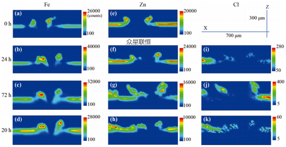
Figure 7. Confocal micro-XRF elemental distribution results of the corrosion process of a hot-dip galvanized steel sheet in NaCl solution.
This experiment is not a direct semiconductor thin film case, but it demonstrates an important capability: X-rays can penetrate the liquid layer, and the polycapillary confocal structure can confine the analysis volume to the vicinity of the target interface. The researchers recorded in real time the loss of the Zn coating and the distribution changes of corrosion-related elements such as Fe and Cl. For semiconductor thin film research, this type of method is more suitable as a capability expansion for wet processing, electroplating, interfacial reactions, and material reliability studies, rather than being simply equivalent to in-line production inspection.
The Ultimate Challenge of Sub-nanometer Ultra-thin Layers:
InAs/GaAs Semiconductor Heterostructures
In semiconductor optoelectronic devices such as quantum dots and superlattices, ultra-thin layers, wetting layers, or interfacial layers with thicknesses below 1 nm can significantly affect the band structure, strain state, and device performance. Non-destructive quantitative analysis of such structures is one of the most difficult tasks in thin film characterization and best demonstrates the technological boundary. Conventional SEM-EDS is susceptible to continuous background and weak peak overlaps, while WDX, although highly sensitive, involves greater system complexity and testing requirements.
Researchers from the University of Sheffield in the UK and Bruker Nano Analytics compared EDX, WDX, and a μXRF system equipped with a polycapillary focusing X-ray source in an SEM[6]. Polycapillary optics focus X-rays from a high-voltage X-ray tube to a few microns in scale, enabling the SEM platform to not only rely on electron beam excitation for EDX/WDX, but also introduce an independent micro-area XRF excitation channel. It should be accurately stated that this study did not prove that μXRF outperforms WDX in all metrics; the paper notes that WDX has the best sensitivity due to its low background. However, the advantage of μXRF lies in providing a new X-ray excitation path within the SEM, which, combined with a high-voltage X-ray tube and polycapillary focusing, can reliably detect and quantify sub-nanometer semiconductor layers.
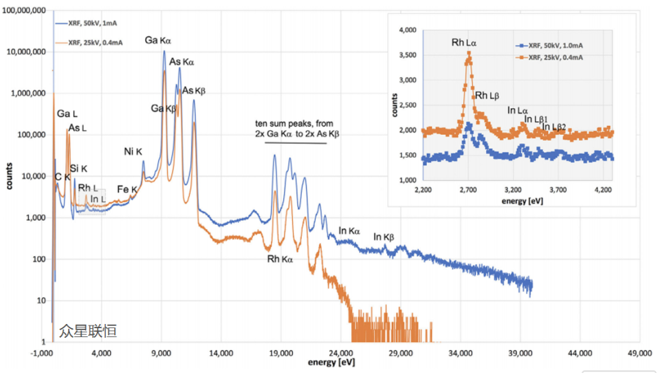
Figure 8. μXRF spectral data of the InAs-on-GaAs sample at 25 kV and 50 kV. The upper right inset shows an enlarged view of the 2.2–4.2 keV region around the Rh-L and In-L lines.
The研究对象 was a 0.8 nm InAs ultra-thin layer deposited on a GaAs(001) substrate. EDX, WDX, and μXRF were all able to detect and quantify the In-L line signal, with μXRF giving an InAs thickness of approximately 0.8 ± 0.2 nm, consistent within error with the results of the other methods. The authors noted that this was, to their knowledge, the first time μXRF was used in an SEM to reliably detect and analyze a sub-nanometer surface layer. In the progressive logic of this article, this case precisely brings the high-throughput micro-area excitation, low-background analysis, and thin film quantification capabilities mentioned in the previous sections back to the characterization of semiconductor ultra-thin heterostructures.
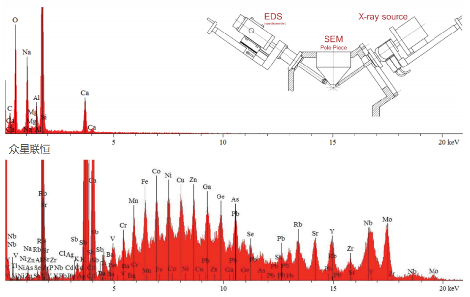
Figure 9. Schematic comparison of the excitable/detectable elemental range between SEM-EDS and an add-on μXRF module.
Furthermore, coupling a μXRF module with polycapillary optics in an SEM is not intended to replace EDX or WDX, but to add an X-ray excitation path to electron microscopy analysis. Electron beam analysis has advantages in light elements, surface sensitivity, and high spatial resolution; μXRF, on the other hand, can more effectively excite certain higher-energy spectral lines using a high-voltage X-ray tube and reduce the impact of the electron beam's continuous background on weak peak identification. For semiconductor thin films and microelectronic materials containing heavy elements, thick packaging layers, metallic interconnects, or buried structures, this complementarity has practical significance.
Summary
In summary, from the calibration of confocal micro-XRF systems and depth profiling of multilayer coatings, to three-dimensional imaging of multilayer coatings, low-background detection of small particles, in-situ observation of solid/liquid interfaces, and finally the μXRF analysis of 0.8 nm InAs/GaAs semiconductor ultra-thin layers, these studies together form a clear capability chain: semiconductor thin film characterization requires not just a single instrument metric, but the combined cooperation of high-throughput micro-area excitation, spatially selective detection, low-background spectral acquisition, and reasonable algorithms/models.
In this capability chain, polycapillary X-ray lenses play the key role of "turning a laboratory X-ray source into a usable micro-area probe." XOS, as an important manufacturer in the field of polycapillary optics, has its polycapillary optics widely used in commercial instruments and various customized X-ray analysis systems, serving fields such as microelectronics, semiconductor manufacturing, materials science, pharmaceuticals, and life sciences.
As a long-term strategic partner and general agent of the U.S. XOS company in the Chinese and Southeast Asian markets, Top Unistar aims not only to introduce a component, but to help users weigh "light source, lens, detector, sample environment, and analysis target" within the same system. For semiconductor thin films, advanced coatings, and microelectronic material testing, truly valuable solutions often come from the matching of these details.
WeBeijing Top Unistar Technology Co., Ltd.understand the working principles of capillary X-ray lenses, performance simulation, and their coupling requirements with X-ray sources, and can provide specification recommendations, customized solutions, engineering integration support, and testing and verification services for users across different application scenarios such as two-dimensional diffraction XRD, parallel beam XRD, XRF, full-field microscopy, extreme ultraviolet spectroscopy, and neutron collection. Putting every X-ray photon in a more appropriate place is also the most fundamental and important value of polycapillary X-ray lenses in advanced thin film characterization.
Related Reading
Measuring Coating Thickness with Polycapillary X-ray Lenses
BioRxiv / Focused X-ray Luminescence Computed Tomography Imaging Using Continuous Scanning Scheme
References
[1] Smolek, S., et al. "Comparison of two confocal micro-XRF spectrometers with different design aspects." X-Ray Spectrometry 43.2 (2014): 93-101.
[2] Nakano, Kazuhiko, et al. "Depth elemental imaging of forensic samples by confocal micro-XRF method." Analytical Chemistry 83.9 (2011): 3477-3483.
[3] Nakano, Hitomi, et al. "Improvement of detection limits for particle contamination by confocal configuration in X-ray fluorescence microscope." Analytical Sciences 37.10 (2021): 1447-1451.
[4] Tsuji, Kouichi, et al. "Development of confocal micro X-ray fluorescence instrument for depth analysis of liquid-solid interface." Analytical Sciences 24.1 (2008): 99-103.
[5] Akioka, Koji, et al. "Depth elemental imaging during corrosion of hot-dip galvanized steel sheet by confocal micro XRF analysis." Analytical Sciences 36.1 (2020): 55-59.
[6] Walther, Thomas, et al. "Comparison of different X-ray-based scanning electron microscopy methods to detect sub-nanometre ultra-thin InAs layers deposited on top of GaAs." Journal of Microscopy (2025).
Content: Jay·Qiu
Proofreading: Kevin
Editing: Sylvia
Disclaimer:
Part of the content (including images) in this article is sourced from the internet. The copyright and views of the quoted parts belong to the original authors. Beijing Top Unistar Technology Co., Ltd. publishes and reposts this content for the purpose of conveying more industry information and network sharing. If you believe this article contains infringing content, please contact us, and we will address it promptly. If you have any questions, please feel free to contact us.
Reprints are welcome; please indicate the source.
FROM READING TO APPLICATION
Put this knowledge to work
Need to assess product suitability, discuss experimental conditions or find technical support? Explore our products and services, or discuss this resource with us.