
CCD output structure
After the last register of the charge‑packet horizontal shift register, the charge packets need to be non‑destructively output in the form of current or voltage.
After the last register of the charge‑packet horizontal shift register, the charge packets need to be non‑destructively delivered in the form of current or voltage.
Output structures include reverse‑biased diode output structure, floating diffusion (FD) output structure, floating‑gate structure, distributed floating‑gate structure, etc. Among them, the floating diffusion (FD) output structure is the most widely used, as shown in the figure below:
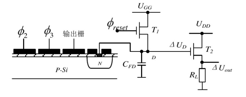
Reset noise will be introduced during the output process.
FROM READING TO APPLICATION
Put this knowledge to work
Need to assess product suitability, discuss experimental conditions or find technical support? Explore our products and services, or discuss this resource with us.