

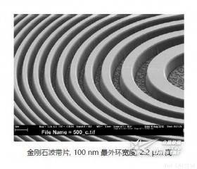
Diamond X-ray Fresnel Zone Plate
The diamond zone plate is specifically designed for high heat load applications at XFEL, allowing a peak power density of 4E17 W/cm2 at the focal point.

Introduction
About XRnanotech
XRnanotech is the result of more than 10 years of research at the renowned Paul Scherrer Institute in Switzerland and was founded in 2020 to bring the latest breakthrough innovations in X-ray optics to market. XRnanotech specializes in the study of nanostructures and the development and manufacture of the most innovative X-ray optical components, achieving the highest resolution, efficiency, stability, and design quality. The product line includes Fresnel zone plates, nanoscale gratings, diamond optical components, nanoresolution test patterns, and 3D resolution test patterns. The Fresnel zone plates manufactured by XRnanotech can achieve resolutions as low as <10 nm, and with the unique Ir-line multiplication technology, X-ray beam focusing can be achieved with precision down to 5 nm, making XRnanotech the world record holder in X-ray lenses.
Product Introduction
Diamond zone plates are specifically designed for high heat load applications at XFEL, allowing a peak power density of 4x10¹⁷ W/cm2 at the focal point.
| Parameters | Typical Values | Capability Limits |
| Outermost Zone Width of Zone Plate [nm] | 100 | 50 |
| Zone Plate Diameter [μm] | 100-250 | >2500 |
Comparison of Material Properties of Gold, Silicon, and Diamond
| Material | Atomic Number | Density [g cm-3] | Melting point [°C] | Thermal conductivity [W m K] | Thickness for π phase shift at 10 keV [µm] |
| Gold, Au | 79 | 19.3 | 1064 | 310 | 2.07 |
| Silicon, Si | 14 | 2.33 | 1410 | 150 | 12.67 |
| Diamond, C | 6 | 3.52 | > 2000 | 2200 | 8.52 |
It can be seen that, thanks to diamond's good thermal conductivity, low X-ray absorption, and high melting point, it is highly suitable for high heat-load applications such as XFEL.
The following shows the irradiation damage test of gold zone plates under FEL:
SEM image of a gold zone plate with 100 nm outermost zone width before irradiation test at LCLS, 8 keV, 1 mJ, 60 Hz pulses
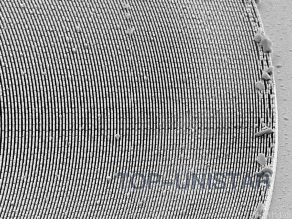
SEM image of a gold zone plate with 100 nm outermost zone width after 1,000 pulses of irradiation test at LCLS, 8 keV, 1 mJ, 60 Hz
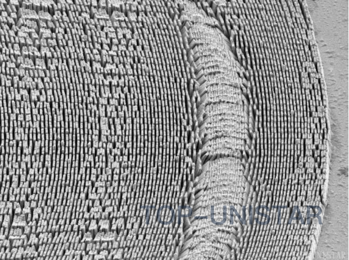
SEM image of a gold zone plate with 100 nm outermost zone width after 10,000 pulses of irradiation test at LCLS, 8 keV, 1 mJ, 60 Hz
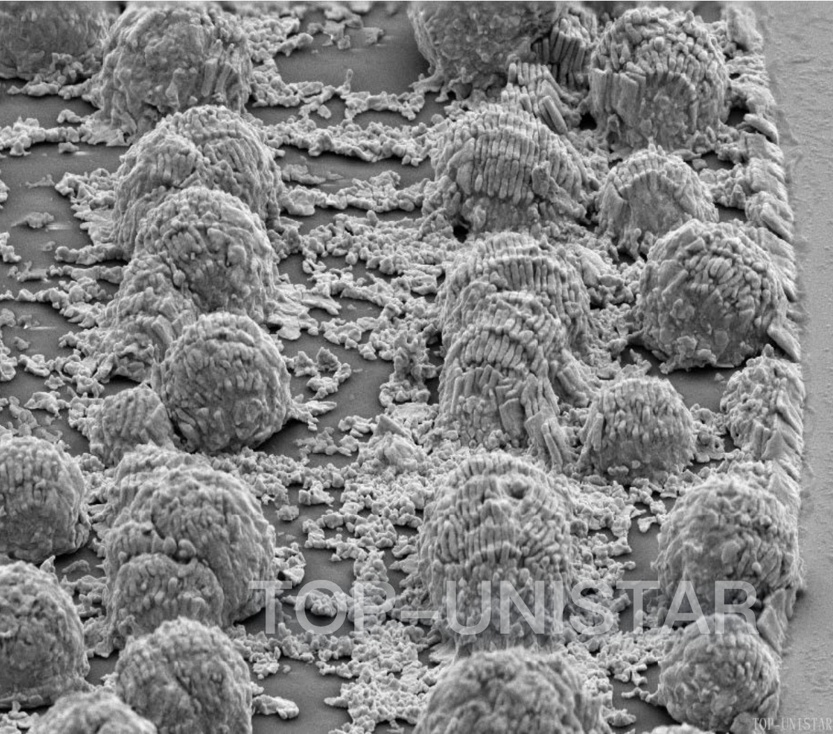
Specifications
| Parameter | Typical value | Capability limit |
| Outermost zone width of zone plate [nm] | 100 | 50 |
| Zone plate diameter [μm] | 100-250 |