
HPC Detector Fabrication

HPC Detector Fabrication Services
As the exclusive distributor of Advacam in China, Top-Unistar jointly offers full-process semiconductor fabrication solutions for photon-counting X-ray detectors, including sensor fabrication wafer bumping, flip-chip bonding, dicing, probing, and sensor/mask design. Leveraging Advacam's mature technologies and facilities, we support domestic HPC detector R&D teams and enterprises to promote photon-counting X-ray detection applications across various fields in China.
Why choose our HPC X-ray detector fabrication services?

Premium Partner Technology & Hardware Infrastructure
Advacam's 2,600 m² cleanroom features complete in-house wafer and flip-chip lines, ensuring strong, integrated semiconductor fabrication capabilities.

Partner with proven technology and a strong track record
Since 2002, Advacam has provided photon-counting detector fabrication to CERN, DESY, and more — delivering consistent, high-quality results with deep process expertise.

Professional market service capabilities
Specialized in photon‑counting detection with responsive local service. Tailored process solutions, trusted long‑term by OEMs and researchers.

Solid foundation in product application implementation
Minipix and Advapix detectors are already deployed in radiation, scattering, and spectral imaging applications in China, supporting fabrication services for diverse experimental needs.


Sensor Fabrication
● Service Scope: 6/8" high-resistivity silicon wafer processing — conventional and micron ultra-thin sensors, planar and edgeless Si devices. Flip-chip/wire bonding, p-stop/p-spray processes for low leakage and high-voltage tolerance. Full modular processing for edgeless devices. ● Applications: Custom silicon sensor R&D for photon-counting X-ray detectors — tailored to thickness, polarity, and active area specifications.

Wafer Solder Bumping
● Service Scope: 6–8" wafer UBM solder bumping (high/low-temp alloys), compatible with Si, GaAs, CdTe sensors. Full electroplating process: cleaning, lithography, plating, reflow — custom solder formulations available. ● Applications: Bump deposition for photon-counting X-ray detector R&D — fitting flip-chip bonding needs for various sensor materials in production and development.

Flip-Chip Bonding
● Service Scope: Standard and custom flip-chip bonding — compatible with Si, GaAs, CdTe sensors to CMOS chips. Tailored processes for Cu TSV chips reduce high-end chip loss. Serves both R&D and commercial production. ● Applications: Hybrid pixel detector flip-chip bonding — for both production-scale manufacturing and custom R&D needs.

Wafer Dicing
● Service Scope: Custom diamond-blade dicing with non-standard cutting capabilities. Slow feed and step-cutting optimize quality, preventing micro-cracks and leakage current in sensor wafers. ● Applications: Precision dicing of photon-counting X-ray detector sensor wafers and CMOS chips — ideal for guard ring structures, ultra-thin sensors, and other high-precision requirements.

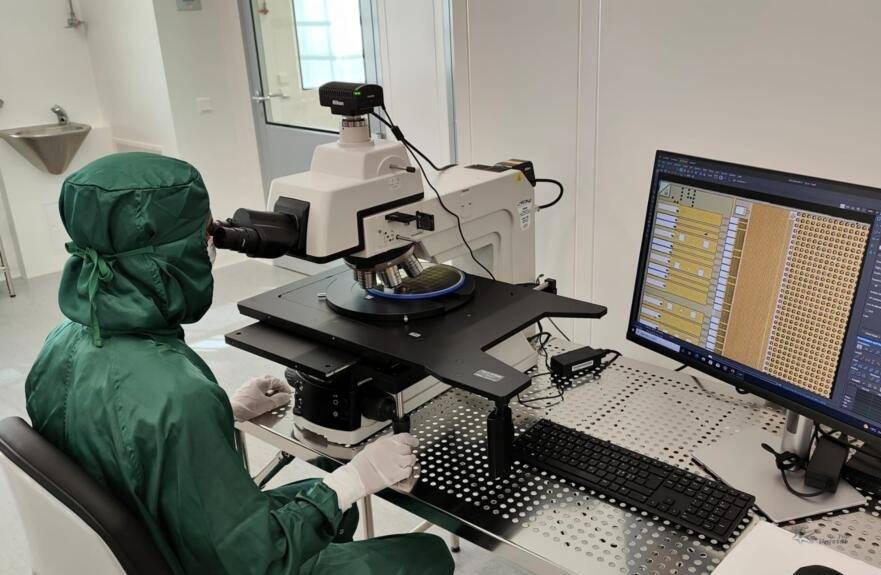
Timepix Readout Chip Detection
● Service Scope: Automated Timepix readout chip probing for sorting and screening. ● Applications: Pre‑screening in photon‑counting detector R&D — works with bumping to minimize contamination and cut costs.

Sensor & Mask Design
● Service Scope: Custom sensor design (contacts, guard rings) with mask design — GDS layout output, flip‑chip compatible. ● Applications: Novel sensor R&D for photon‑counting detectors — for projects requiring customized performance.